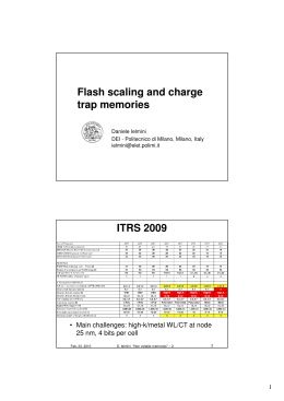
Phase change memories Daniele Ielmini DEI - Politecnico di Milano, Milano, Italy [email protected] Flash scaling overview 1. Flash scaling: T. Kamaigaichi, et al., IEDM Tech. Dig. 2008 www.micron.com Feb. 26, 2010 2. Evolutionary scenario: H. Tanaka et al., VLSI Symp. 2007 3. Paradigm shift M. Lee, et al., IEDM Tech. Dig. 2007 D. Ielmini, "Non volatile memories" – 3 2 1 Outline • PCM storage concept • Program/erase characteristics • Reliability • Program disturb • Endurance • Crystallization • Structural relaxation • Scaling perspective • Conclusions Feb. 26, 2010 3 D. Ielmini, "Non volatile memories" – 3 Phase change memory (PCM) WL WL plug BL1 BL2 BL3 BL4 c h c h W W p+ p+ n c h c h W W p+ p+ p R. G. Neale, D. L. Nelson, N. Carlisle, “The and G. E. Moore, Ovshinsky invention,” “Nonvolatile and Science & Mechanics, Reprogrammable, the ReadFeb. 1970 Mostly Memory is Here,” Electronics, Sep. 1970 F ≈ 2 mm 1 bit Feb. 26, 2010 F ≈ 350 µm 256 bit D. Ielmini, "Non volatile memories" – 3 G. Servalli, “A 45nm generation phase change memory technology,” IEDM Tech. Dig. 2009 F ≈ 52 nm 1 Gbit 4 2 Storage concept IVA VA VIA VIIA C N O F Si P S Cl Crystalline (set state) Ge As Se Br Amorphous (reset state) Sn Sb Te I Pb Bi Po At Feb. 26, 2010 5 D. Ielmini, "Non volatile memories" – 3 PCM concept Top contact c-GST Temperature Bottom contact a-GST Tm Time Feb. 26, 2010 D. Ielmini, "Non volatile memories" – 3 6 3 PCM logic states 10 10 Current [A] Top contact c-GST c-GST Bottom contact Reset state a-GST 10 10 10 -4 Set state -5 VT -6 Reset state -7 R=V/I -8 10 Ge2Sb2Te5 -9 0 0.2 0.4 0.6 0.8 1 1.2 1.4 Voltage [V] Set state Feb. 26, 2010 D. Ielmini, "Non volatile memories" – 3 7 Cell structure Cell Structure: selector (T) + storage element (R) = 1T1R Transistor: • BJT • MOSFET Bit line Word line Bit line Storage element Word line Selector Feb. 26, 2010 Resistor: heater/material • Heater – Sub-litho contact – µTrench – Planar options • Material – GST, AIST, SbTe, … D. Ielmini, "Non volatile memories" – 3 8 4 MOSFET-selected PCM cell BL GND WL n+ p-substrate n+ • • • • STI • Feb. 26, 2010 Larger cell size: 18-40 F2 Scalable ? Minimum mask overhead Suitable for low-cost embedded applications, medium-low size memories Easier array design D. Ielmini, "Non volatile memories" – 3 9 BJT-selected PCM cell WL BL p+ n+ n-well p-substrate WL WL plug BL1 BL2 BL3 BL4 c h c h c h c h W W W W p+ p+ n • Better current driving capabilities • Compact integration suitable for high-density applications: 8-10 F2 and scalable • Dedicated process module for BJT formation, more complex array design p+ p+ p Feb. 26, 2010 D. Ielmini, "Non volatile memories" – 3 10 5 Diode-selected PCM cell • Good current driving capabilities • Extremely compact integration suitable for ultra-high-density applications: 4-5 F2 • Diode must provide high forward (reset) current and low subthreshold (leakage) current poly-Si diode demonstrated Scalable? Stackable? BL p+ n+ WL • Hitachi, VLSI 2009 Feb. 26, 2010 11 D. Ielmini, "Non volatile memories" – 3 Basic cell structure Top-view Planar heater + confined GST = pore Metal GST Oxide Heater Cross-section Confined heater + planar GST = lance Metal GST Oxide Oxide Oxide Heater Metal Metal GST-Heater Interface GST Feb. 26, 2010 Heater D. Ielmini, "Non volatile memories" – 3 12 6 Lance structures Samsung 2003 Intel 2006 IBM 2008 Metal GST Heater STMicroelectronics 2006 Feb. 26, 2010 D. Ielmini, "Non volatile memories" – 3 13 Pore structures (A) Ireset=700µA @180nm Samsung CVD 2007 IBM 2007 Feb. 26, 2010 Samsung ‘recess’ 2003 Samsung ‘dash’ 2003 D. Ielmini, "Non volatile memories" – 3 IBM ‘pillar’ 2007 14 7 Line structure Philips 2004 IBM 2006 Nasa 2008 NXP 2007 Feb. 26, 2010 15 D. Ielmini, "Non volatile memories" – 3 Technology benchmarking STMIntel Samsung Hitachi IBMNumonyx QimondaMacronix Hitachi Year 2006 2006 2006 2007 2009 2009 F [nm] 90 90 130 180 45 80 Cell type µtrench/ lance, bipolar, Ring, GST N-doped, epi-Si diode Lance, GST Ta2O5 layer, MOSFET Pore, GST Ndoped MOSFET Wall, bipolar Pillar, poly-Si diode, crossbar Ireset [µ µA] 400/700 600 100 400 200 160 Array size [# bit] 128M 512M 4M 256k 1G Cell size [F2] 6 106 105 Endurance [#] >108 Feb. 26, 2010 5.8 5.5 105 D. Ielmini, "Non volatile memories" – 3 4 109 16 8 • PCM storage concept • Program/erase characteristics • Reliability • Program disturb • Endurance • Crystallization • Structural relaxation • Scaling perspective • Conclusions Feb. 26, 2010 17 D. Ielmini, "Non volatile memories" – 3 Set/reset in PCM devices IT Im Ix Reset Set A. Redaelli, et al., IEEE EDL 2004 • IT < I < Ix no change (switching ≠ crystallization!) • Ix < I < Im crystallization • I > Im melting + quenching Feb. 26, 2010 D. Ielmini, "Non volatile memories" – 3 18 9 Set characteristics 6 Resistance [Ω] 10 tset 5 10 10 µs 250 ns 100 ns 40 ns 20 ns 4 10 3 10 0 100 200 300 400 500 600 Programming Current [µA] Set with < 100 ns pulses still maintaining good reading window Feb. 26, 2010 19 D. Ielmini, "Non volatile memories" – 3 Reset characteristics • FEM modeling of: – Conduction (drift-diffusion) – Heating (Joule power dissipation, heat conduction) 10 Data Calculations 800 Resistance [Ω] Current [µA] 1000 Ron 600 400 200 0 Rset 0 Feb. 26, 2010 0.5 Voltage [V] 1.5 2 I 7 10 10 10 10 1 V Data Calculations 6 5 4 Rset Im 3 0 200 400 600 800 1000 1200 Current [µA] D. Ielmini, "Non volatile memories" – 3 20 10 Melting condition GST melting temperature, Tm Resistance [Ω] 10 Cryst. GST 7 Data Calculations 6 10 program 5 10 melting 4 10 3 10 Amorphous GST Feb. 26, 2010 0 200 400 600 800 1000 1200 Current [µA] D. Ielmini, "Non volatile memories" – 3 21 Constant Rset optimization Lc Lh φ 3 degree of freedom for minimizing Im: Chalcogenide height, Lc Heater height, Lh Contact diameter, φ Feb. 26, 2010 Fixed φ (technology), Rset (readout) 1 degree of freedom (Lh or Lc) D. Ielmini, "Non volatile memories" – 3 22 11 Ireset optimization 1200 φ=30nm Im [µA] 1000 800 600 400 200 0 Feb. 26, 2010 Rset = 3 kΩ Rc,Rcth 50 100 150 Lh [nm] Rh,Rhth 23 D. Ielmini, "Non volatile memories" – 3 Program-read tradeoff 1200 φ=30nm Im [µA] 1000 800 2 kΩ 600 3 kΩ 400 4 kΩ Rset=5 kΩ 200 0 Feb. 26, 2010 50 100 Lh [nm] D. Ielmini, "Non volatile memories" – 3 150 24 12 Scaling of R, I, V I∝F I ∝ F1.3 Feb. 26, 2010 25 D. Ielmini, "Non volatile memories" – 3 Ireset scaling Pore 100000 Lance 100000 Lance/C60 DCC IBM pillar Samsung CVD I∝ A0.5 Samsung dash I∝ A0.65 ITRI cross spacer IBM keyhole 100 Hitachi crossbar 10 1000 100000 Area [nm2] Feb. 26, 2010 Hitachi Wplug Hitachi O-doped STM utrench 1000 I ∝ A0.5 Intel lance I ∝ A0.65 100 Samsung Ndoped lance Numonyx wall itrs 2009 itrs 2009 itrs 2007 itrs 2007 Samsung dash 2 10 Samsung lance 10000 Ireset [µA] Ireset [µA] Ovonycs pore 1000 lance w/o C60 CC 10000 Samsung ring 10 10 1000 100000 STM utrench Area [nm2] D. Ielmini, "Non volatile memories" – 3 26 13 • PCM storage concept • Program/erase characteristics • Reliability • Program disturb • Endurance • Crystallization • Structural relaxation • Scaling perspective • Conclusions Feb. 26, 2010 D. Ielmini, "Non volatile memories" – 3 27 PCM reliability issues Reliability issue Cell impact Program disturb Resistance decrease/increase Cycling endurance Stuck set/reset Structural relaxation Resistance increase Crystallization Resistance decrease Read disturb Switching, resistance decrease Noise Resistance fluctuation Feb. 26, 2010 D. Ielmini, "Non volatile memories" – 3 28 14 Program disturb RC1 R12 RC2 Chalcogenide Heater Insulator Feb. 26, 2010 RH1 RH2 29 D. Ielmini, "Non volatile memories" – 3 Cycling endurance K. Kim and S. J. Ahn, IRPS 2005 Stuck set Feb. 26, 2010 Stuck reset D. Ielmini, "Non volatile memories" – 3 30 15 Stuck-set mechanism Before After cycling B. Rajendran, et al., VLSI Tech. Dig. 96, 2008 Feb. 26, 2010 D. Ielmini, "Non volatile memories" – 3 31 Crystallization Feb. 26, 2010 D. Ielmini, "Non volatile memories" – 3 32 16 Nucleation/growth (N/G) − Nucleation rate Growth velocity IN = IN0e ∆GA +∆G* kBT ∆G − A kBT ∆G* = 16πσ 3 2 3∆GV vG = vG0e • ∆GA: barrier for atomic motion (constant) • ∆G*: barrier for the formation of a stable nucleus (increases with T melting point) Feb. 26, 2010 D. Ielmini, "Non volatile memories" – 3 33 Evidence for nucleation S.-H. Lee, et al., Nano Lett. 8, 3303 (2008) Feb. 26, 2010 D. Ielmini, "Non volatile memories" – 3 34 17 Evidence for growth Y. H. Shih, et al., IEDM Tech. Dig. (2008) Feb. 26, 2010 35 D. Ielmini, "Non volatile memories" – 3 Cumulative distrib. % Percolation model 99 75 50 25 10 3 1 o 190 C 180 C rC=2.2nm 3.3nm 5.6nm 10 Feb. 26, 2010 o o T=210 C 0 10 1 10 2 10 3 Retention lifetime [s] D. Ielmini, "Non volatile memories" – 3 10 4 36 18 tX extrapolation o T [ C] 300 200 10 years tX [s] 10 10 10 100 70 8 ∆G 10 150 Arrhenius 6 o T10Y=118 C 4 EX 2 τ = τ x0 e Data Calculated Reaction coordinate 0 10 20 25 30 EX = 2.5 eV τx0 = 10-23 s ??????? 35 -1 Ex kT 1/kT [eV ] U. Russo, et al., IEEE T-ED 54, 2007 Feb. 26, 2010 37 D. Ielmini, "Non volatile memories" – 3 R drift – atomic relaxation 6 10 o R [Ω] 9x10 8.5x10 8x10 7.5x10 5 T=25 C ∆G 9.5x10 5 5 ν 5 t R = R0 t0 5 5 7x10 0 10 1 2 10 10 τ = τ0e EA kT EA Reaction coordinate 3 10 Time [s] D. Ielmini, et al., IEEE T-ED 56, 2009 Feb. 26, 2010 D. Ielmini, "Non volatile memories" – 3 38 19 SR data S. Roorda et al., PRB 44, 3702, 1991 Ishimaru et al., PRL 2002 SR K. Koughia et al., JAP 2005 J. A. Mullin, PhD thesis, 2000 Mechanism = thermally-activated defect annihilation Feb. 26, 2010 39 D. Ielmini, "Non volatile memories" – 3 Kinetic model for SR Distributed EA: Energy NT EA EA τ = τ0e Monomolecular dynamics: EA kT Reaction coordinate dN(E NT T A) =dt τ(E A ) D. Ielmini, et al., IEDM Tech. Dig. 2007 Feb. 26, 2010 D. Ielmini, "Non volatile memories" – 3 40 20 Why distributed EA? • Single EA level NT R Energy EA τ = τ0e • EA distribution NT EA kT time R Energy Feb. 26, 2010 time D. Ielmini, "Non volatile memories" – 3 41 Simulation results: R vs. t Initial t =10s 102 s 103 s Activation energy [eV] T = 300 K Feb. 26, 2010 D. Ielmini, "Non volatile memories" – 3 42 21 Temperature dependence 9 10 o 90 C o 110 C o 130 C o 170 C o 180 C 8 R [Ω] 10 7 10 R* Power-law extrapolations Crystallization 6 10 5 10 -6 -5 -4 -3 -2 -1 0 1 2 3 4 5 6 10 10 10 10 10 10 10 10 10 10 10 10 10 Time [s] Feb. 26, 2010 43 D. Ielmini, "Non volatile memories" – 3 Arrhenius plot o T [ C] 10 10 8 10 6 10 4 τSR [s] 10 2 10 500 300 200 R* = 5 MΩ 10 MΩ 20 MΩ 50 MΩ 100 MΩ 200 MΩ τX 100 R* 0 10 10 10 10 -2 TMN = 760 K -4 -6 -8 10 10 15 20 25 30 35 -1 1/kT [eV ] Feb. 26, 2010 D. Ielmini, "Non volatile memories" – 3 44 22 Meyer-Neldel rule • Arrhenius law with distributed EA E τ SR =τ 0 exp A kT • Crossing at TMN pre-exponential τ0 is not constant, but is an exponential function of EA Meyer-Neldel (MN) rule EA kTMN τ 0 =τ 00 exp − Feb. 26, 2010 N 45 D. Ielmini, "Non volatile memories" – 3 Analytical model for R drift 1 ν • From t R = R0 t0 we obtain τ SR E EA − A R* ν kT = t0 = τ e e kTMN 00 R0 • Then the power-law exponent is given by: 0.35 0.3 EA = k α Data Calculated 0.25 1- T TMN log ( R* R 0 ) ν [1] ν= αT 0.2 0.15 0.1 0.05 0 250 300 350 400 450 500 T [K] Feb. 26, 2010 D. Ielmini, "Non volatile memories" – 3 46 23 Unified kinetic model • •Almost Relaxation identical and behavior crystallization displayed are by completely described different by the same systems Arrhenius (a-Si, law metallic + glasses) Meyer-Neldel rule τ = τ0e EA kT - τ 0 = τ 00 e EA kTMN [s] ττ00[s] 0 -4 10 10-5 -6 10 10 -10 10 -8 10 -15 10 -10 10-20 10 -12 10-25 10 -14 -30 10 10 -16 -35 10 10 -18 -40 10 10 -45 -20 10 10 -50 -22 10 10-55 -24 10 10-60 -26 10 10 00 [1] R. S. Crandall, PRB 1991 Relaxation Crystallization [2] V. A. Khonik, et al., JAP 2000 Calculated GST relaxation GST crystallization a-Si:H [1] Metallic glasses [2] 10.52 13 4 5 2 6 2.5 7 1.5 83 [eV] D. Ielmini and M. Boniardi, APL 2009 EEAA[eV] Feb. 26, 2010 47 D. Ielmini, "Non volatile memories" – 3 T-acceleration model To normalize SR time to a given T: t 1 =τ β= T2 T β 2 T1 T1 00 2 1− β t TMN − T1 TMN − T2 T1 = 25°C Feb. 26, 2010 D. Ielmini, "Non volatile memories" – 3 48 24 Unified energy landscape 10 ∆G Crystallization 10 -6 10 Noise SR 10 τ0 [s] E’A -4 10 -8 Noise -10 -12 -14 10 -16 10 EA 10 EX RTN data SR data [6] Cryst. data [6] 10 10 SR -18 -20 -22 Crystallization -24 10 0 0.5 1 1.5 2 2.5 3 Activation Energy [eV] • • • Noise: D. Fugazza, et al., IRPS 2010 SR: D. Ielmini and M. Boniardi, APL 2009 Crystallization: A. Redaelli, et al., IEDM Tech. Dig. 2005 Feb. 26, 2010 49 D. Ielmini, "Non volatile memories" – 3 Reliability issues: 1/f noise 12 VBias = 66mV 4 τ12 0 τ21 -4 ∆G Current [nA] 8 -8 0.00 0.05 0.10 0.15 0.20 0.25 Time [s] Reaction coordinate Feb. 26, 2010 D. Ielmini, "Non volatile memories" – 3 50 25 Structural relaxation 6 10 o 8.5x10 8x10 7.5x10 T=25 C ν R=R0(t/t0) 5 5 5 5 5 7x10 0 10 1 2 10 10 3 10 Time [s] Reaction coordinate Feb. 26, 2010 D. Ielmini, "Non volatile memories" – 3 51 Crystallization ∆G R [Ω] 9x10 5 ∆G 9.5x10 Reaction coordinate Feb. 26, 2010 D. Ielmini, "Non volatile memories" – 3 52 26 • PCM storage concept • Program/erase characteristics • Reliability • Program disturb • Endurance • Crystallization • Structural relaxation • Scaling perspective • Conclusions Feb. 26, 2010 D. Ielmini, "Non volatile memories" – 3 53 Fast/slow cells EA = 3.2 eV EA = 2.7 eV • Retention time correlation material non-uniformity in the array resulting in systematically fast/slow cells D. Mantegazza, et al., IEDM Tech. Dig. 2008 Feb. 26, 2010 D. Ielmini, "Non volatile memories" – 3 54 27 Impact on scaling • Cell downscaling results in larger variability of fast/slow crystallization Feb. 26, 2010 55 D. Ielmini, "Non volatile memories" – 3 o Tx [ C] Size-dependent crystallization 1000 800 600 500 400 300 Si nanodot [1] GeSb nanodot [2] 200 GeSbTe nanowire [3] 100 0 10 1 10 2 10 D [nm] S. Raoux, et al., MRS 2008 [1] Hirasawa et al., APL 2006, [2] Raoux et al., EPCOS 2007, [3] Lee et al., Nature Nanotech., 2007 • 1D scaling (film) growth constriction? • 2D scaling (nanowire) surface oxidation/depletion? • 3D scaling (nanodot) true PCM-like scaling (isotropic) Feb. 26, 2010 D. Ielmini, "Non volatile memories" – 3 56 28 Material engineering X. S. Miao, et al., Jap. J. Appl. Phys. 2006 Amplitude [a.u.] Y. C. Chen, et al., IEDM Tech. Dig. 2006 y/(x+y) 0 T. Morikawa, et al., IEDM Tech. Dig. 2007 Feb. 26, 2010 50 100 150 200 250 300 350 Temperature [°C] Wavelength [nm] N. Yamada, et al., J. Appl. Phys. 1980 D. Ielmini, "Non volatile memories" – 3 57 Conclusions • Outstanding endurance promising for RAM applications • Reduction of reset current requires sublitho cell area scaling • Best Ireset reduction conflicts with thermal cross-talk • Reliability impacts on high-T applications (automotive) and MLC (resistance drift) Feb. 26, 2010 D. Ielmini, "Non volatile memories" – 3 58 29
Scaricare