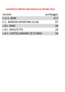
Poltecnico di Bari
15th International Conference on
Transparent Optical Networks
Cartagena, Spain, June 23-27, 2013
Photonic components for signal
routing in optical networks on chip
Vincenzo Petruzzelli, Giovanna Calò
Dipartimento di Elettronica ed Elettrotecnica, Politecnico di Bari
Via Re David, 200 - 70125 Bari
Phone (39) 080-5963645 - Fax (39) 080-5963410 - e-mail: [email protected]
OUTLINES
Poltecnico di Bari
Progress in silicon based technology
Why rapid development of the Integration of
Photonics networks on chip?
1D PBG devices for wavelength division
multiplexing applications on photonic networks
on chip
2D PBG devices for wavelength routing in
photonic networks on chip
Conclusions
Why Silicon Photonic Technology?
Poltecnico di Bari
Silicon can be considered the workhorse of the
semiconductor industry
Due to its abundance and versatility the silicon can be
regarded as a dominant platform for the
microelectronic fabrication
Crystalline silicon photonic waveguides are capable
of transporting wavelength-parallel optical data with
terabit per second data rates across the entire chip
Silicon waveguides can be bent, crossed and coupled,
creating regions where the optical signal can be
passed from one waveguide to another one
Why Optical Interconnects?
Poltecnico di Bari
The recent (i.e. since 2006) advances in:
Massive fabrication of silicon photonic devices
Integration of silicon photonic devices in CMOS
electronic circuits
photonic technology practical for a new generation of NoCs.
Advantages of photonic NoCs:
High transmission bandwidth
Low power consumption
Low latency
Integration of Photonic Networks on chip - NoC
Poltecnico di Bari
SUPERCOMPUTING BOARD
Photonic
Network
CMP stack
DRAM
Memory
CMP
Chip MultiProcessor
[1] A. Biberman, K. Bergman, Rep. Prog. Phys. 75 (2012) 046402
Photonic Building Blocks
Photonic NoC
Poltecnico di Bari
High speed Modulators
Photodetectors
[2] L. Chen, Michal Lipson, Optics
Express, Vol. 17, Issue 10, pp. 79017906 (2009)
10 – 40 Gb/s
[1] Q. Xu et Al., Optics Express, Vol. 15,
Issue 2, pp. 430-436 (2007)
SWITCH MATRIX for the signal routing all over the network
Basic elements: Switches, filters, etc.
SOI WAVEGUIDES
2.8
w
Si
y
d
SiO2
x
Effective refractive index
Poltecnico di Bari
2.6
2.4
w2
d=200 nm
2.2
2
w1
1.8
1.6
1.4 0
0.1
0.2
0.3
0.4
Width w [µm]
Periodic effective
refractive index by
varying the waveguide
width w
1D PBG WAVEGUIDE
0.5
0.6
1D PBG WAVEGUIDE
SiO2
Poltecnico di Bari
w1
w2
l1 l
2
d
Bragg Wavelength
Si
λB = 2 ( neff 1l1 + neff 2 l2 )
PBG: ∆λ ≅ 300 nm
1.55 µm
Si core refractive index
3.477
SiO2 substrate and cladding refractive index
1.444
Waveguide depth d
200 nm
Width of the first layer w1
500 nm
Width of the second layer w2
260 nm
Length of the first layer l1
180 nm
Length of the second layer l2
0.180 µm
Number of layers N
32
1
T
0.9
Transmittance, Reflectance
Bragg wavelength
0.8
0.7
0.6
0.5
0.4
0.3
0.2
0.1
0
1.3
R
1.4
1.5
1.6
1.7
wavelength λ [µm]
1.8
1D PBG WAVEGUIDE with 1 DEFECT
Ld
Poltecnico di Bari
z
1
0.9
0.9
R
Transmittance, Reflectance
Transmittance, Reflectance
1
0.8
0.7
0.6
0.5
0.4
0.3
0.2
T
0.1
0
1.3
1.4
1.5
1.6
1.7
Wavelenght λ [um]
Ld=2l2=0.360 µm
1 channel
1.8
0.8
R
0.7
0.6
0.5
0.4
0.3
T
0.2
0.1
0
1.3
1.4
1.5
1.6
1.7
Wavelenght λ [um]
Ld=10 µm
6 channels
1.8
1D PBG WAVEGUIDE with 1 DEFECT
Defect length variation
160
35
140
30
120
FSR [nm]
40
25
100
20
15
80
60
10
40
5
20
00
10
20
30
defect length [µm]
40
00
50
10
20
18
Channel bandwidth [nm]
number of channels
Poltecnico di Bari
16
14
12
10
8
6
4
2 0
10
20
30
defect length [µm]
40
50
20
30
40
defect length [µm]
50
1D PBG WAVEGUIDE with 2 DEFECTS
Defects
Poltecnico di Bari
Def2
Def1
M-m
1
Nt1
N
Nt1
Nt2
1.7
1
m=2
m=4
m=8
0.9
1.65
Wavelength λ [µm]
0.8
Transmittance T
M+m
M=N/2
0.7
0.6
0.5
0.4
0.3
0.2
1.6
1.55
1.5
1.45
0.1
0
1.3
1.4
1.5
1.6
1.7
Wavelength λ [µm]
1.8
1.4
0
2
4
6
8
10
Defect position index m
12
14
BINOMIAL DISTRIBUTION of DEFECTS
16
16
Poltecnico di Bari
(a)
8
16
8
(b)
12
4
12
4
(c)
8
2
12
8
2
(d)
1
2 BINOMIAL DEFECTS
2 defecst
1 defect
0.9
Transmittance T
0.8
Ld=2l2=0.360 µm 1 channel
0.7
0.6
0.5
Channel bandwidth [nm]
0.4
0.3
0.2
0.1
0
1.3
1.4
1.5
1.6
1.7
Wavelength l [um]
1.8
1 defect
41.5
2 binomial defects
101.5
BINOMIAL DISTRIBUTION of 2 DEFECTS
Poltecnico di Bari
Ld=10 µm
6 channels
0.9
0.9
0.8
0.8
0.7
0.7
Transmittance T
Transmittance T
1
0.6
0.5
0.4
0.3
0.6
0.5
0.4
0.3
0.2
0.2
2 defects
1 defect
0.1
0
1.3
2 defects
1 defect
1.4
1.5
1.6
1.7
0.1
0
1.55
1.8
1.56
1.57
1.58
1.59
1.6
1.61
Wavelength l [um]
Wavelength λ [µm]
FSR [nm]
Channel bandwidth [nm]
1 defect
43.9
7.4
2 binomial defects
44.2
12.6
λ-Routers for Photonic NoC
Poltecnico di Bari
Principle scheme
Physical scheme
Bend
Waveguide
Crossing
Resonator
Photonic Crystals for the Optical Interconnects
We need:
waveguides
resonators
bends
crossings
NoC Components in Photonic Crystals
FDTD Simulations
Poltecnico di Bari
Bend waveguide
Straight waveguide
Silicon Pillars
NoC Components in Photonic Crystals
Broadband Crossing λ=1.35 µm -1.6 µm
Poltecnico di Bari
FDTD Simulations
OUT
North
Input at South port
Output at North port
W and E are isolated
1
0.9
West
East
transmittance
0.8
0.7
0.6
W
E
N
0.5
0.4
0.3
0.2
0.1
0
1.3
IN
South
1.35
1.4
1.45
1.5
wavelength [µm]
1.55
1.6
1.571
Maximum attenuation A=-0.75 dB at λ=1.571 µm
NoC Components in Photonic Crystals
1x2 Photonic Crystal Ring Resonator Switch
Poltecnico di Bari
North
λ1
OFF resonance λ1
Input South
Output North
ON resonance λ2
Input South
Output East
1
λ2
0.9
λ2
West
0.8
transmittance
East
0.7
λ1
0.6
0.5
E
N
0.4
0.3
0.2
0.1
0
1.3
1.35
1.4
1.45
1.5
wavelength [µm]
IN
South
1.55
1.6
NoC Components in Photonic Crystals
4x4 Photonic Crystal Ring Resonator Switch Matrix
Poltecnico di Bari
In North
OUTPUT
Out North
INPUT
In
East
Out
West
1
W
E
S
0.9
Out
East
transmittance
0.8
In
West
0.7
0.6
0.5
0.4
0.3
Out South
In South
0.2
0.1
0
1.48
1.49
1.5
1.51
1.52
1.53
wavelength [um]
1.54
1.55
Conclusions
Poltecnico di Bari
Silicon components make possible the optical interconnects on
chip.
Photonic crystals on silicon integrated on NoC: to perform
all the operations of the conventional silicon components,
but with more compact sizes.
1D PBG multi-wavelength filters: the Newton binomial
distribution of defects allow flat transmission channels with
larger bandwidth.
2D PhCs for the wavelength routing in photonic networkds
on chip
Scaricare