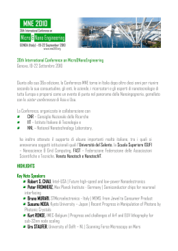
G. Barillaro, A. Diligenti, L. M. Strambini, S.
Surdo
Gruppo Tecnologie Microelettroniche e
Microsistemi
Dipartimento di Ingegneria dell’Informazione
Università di Pisa (I)
Silicon Photonic Crystal Optofluidic
Microsystems for Label-Free
Detection
Collaborations and Available Grants
• Dip. Elettronica, Università di Pavia
– Optical characterization of photonic crystals
• IFAC-CNR, Firenze
– Functionalization of photonic crystals
• Grants
– CARIPLO 2007, “Development of an optical biosensor for the detection
of amyloid fibrils-ligands interactions on a silicon micromachined
structure”, UniPv - UniGe – UniPi
– PRIN-COFIN 2007, “Photonic Crystal Optofluidic Microsystems for
Biosensing”, UniPi - UniPv - IFAC CNR Fi
G. Barillaro
Pisa 28/01/2009
Why Using Photonic Crystals
for Biosensing
• Photonic crystals (PC) are optical structures characterized by
propagation gaps for the EM radiation at certain wavelength ranges
• Optical properties of PCs are highly sensitive to tiny changes of
dielectric constant/thickness of materials composing the structure
• Optofluidic biosensor requires that some portion of the structure
must be in contact with a suitable fluid for surface functionalization/
bioreceptor immobilization
• Photonic crystals obtained by trench formation in a high-refractiveindex material are thus good candidates for optofluidic biosensors
– air in the trench can be replaced with the solution for functionalization/
immobilization of biolayers on the PC internal surface
– changes induced on the PC structure by biolayers can be optically monitored
G. Barillaro
Pisa 28/01/2009
Photonic Crystals@GTMM-UNIPI
• Design, by analytical
calculation (e.g. TMM) and
FEM (e.g. COMSOL) simulation
• Fabrication, by using an
electrochemical
micromachining technology
(ECM)
• Modeling, by analytical
calculation (e.g. TMM) and
FEM (e.g. COMSOL) simulation
G. Barillaro
Firenze 03/04/2009
Photonic Crystals@GTMM-UNIPI
• Design, by analytical calculation
(e.g. TMM) and FEM (e.g.
COMSOL) simulation
• Fabrication, by using an
electrochemical
micromachining technology
(ECM)
• Modeling, by analytical
calculation (e.g. TMM) and FEM
(e.g. COMSOL) simulation
G. Barillaro
Firenze 03/04/2009
Photonic Crystals@GTMM-UNIPI
• Design, by analytical calculation
(e.g. TMM) and FEM (e.g.
COMSOL) simulation
• Fabrication, by using an
electrochemical
micromachining technology
(ECM)
• Modeling, by analytical
calculation (e.g. TMM) and FEM
(e.g. COMSOL) simulation
G. Barillaro
Firenze 03/04/2009
Photonic Crystals@GTMM-UNIPI
• Design, by analytical calculation
(e.g. TMM) and FEM (e.g.
COMSOL) simulation
• Fabrication, by using an
electrochemical
micromachining technology
(ECM)
• Modeling, by analytical
calculation (e.g. TMM) and FEM
(e.g. COMSOL) simulation
G. Barillaro
Firenze 03/04/2009
Publications
– Barillaro G., Diligenti A., Benedetti M., Merlo S., Silicon micromachined
periodic structures for optical applications at l=1.55 m, Applied Physics
Letters, 2006, Vol. 89, Article no. 151110
– Barillaro G., Annovazzi-Lodi V., Benedetti M., Merlo S., Reflection
properties of hybrid quarter-wavelength silicon microstructures, Applied
Physics Letters, 2007, Vol. 90, Article no. 121110
– Barillaro G., Merlo S., Strambini L, Band gap tuning of silicon
micromachined 1D photonic crystals by thermal oxidation, IEEE Journal
of Selected Topics in Quantum Electronics (Special Issue on
Semiconductor Photonic Materials, 2008) 14(4), 2008
– Barillaro G., Strambini L, Annovazzi-Lodi V. Merlo S., Optical
Characterization of High-Order 1D Silicon Photonic Crystals, IEEE Journal
of Selected Topics in Quantum Electronics (Special Issue on
Nanophotonics and Optical Mems, 2009) 15(5), 2009
G. Barillaro
Pisa 28/01/2009
Thank you
Scaricare