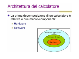
Memory
Memory types
Composition
Hierarchy
Caches
Vahid, Givargis
Introduction
Embedded system’s functionalities can be classified
into processing, storage and communucation
Processing: Transformation of data
Processors
Storage: Retention of data
Memories
Communication: Transfer of data
Buses
Vahid, Givargis
-2-
Basic concepts
Stores large number of bits
Memories are organized in words
An M x N memory
bit
M=2k words
k address input signals
word
N bits per word
E.g.: 4096 x 8 memory:
4,096 x 8 = 32,768 bits
4,096 = 212
12 address input signals
8 input/output data signals
Vahid, Givargis
-3-
Basic concepts
Memory access signals
r/w
enable
Selects read or write
Read or write only when asserted
Memory address/data
A[0..k-1]
D[0..N-1]
Address
Data
r/w
enable
A[0]
A[1]
2k x N
Memory
D[0]
D[1]
D[N-1]
A[k-1]
Vahid, Givargis
-4-
Memory classification
Traditional ROM/RAM distinctions
ROM: Read only, bits stored without power
RAM: Read and write, lose stored bits without power
Traditional distinctions blurred
Advanced ROMs can be written to
PROM, EPROM, E2PROM, FLASH
Advanced RAMs can hold bits without power
NVRAM
Writing
Manner and speed a memory can be written
Storage
Ability to hold stored bits once written
Vahid, Givargis
-5-
Memory classification: Writing
High end
Processor writes to memory simply and quickly (RAM)
Middle range
Processor writes to memory, but slower (FLASH,
E2PROM)
Lower range
A programmer writes to memory (EPROM, OTP ROM)
Low end
Bits stored only during fabrication (ROM)
Vahid, Givargis
-6-
Memory classification: Storage
High end
Essentially never loses bits (ROM)
Middle range
Hold bits months or years after memory’s power
source turned off (NVRAM)
Lower range
Hold bits as long as power supplied to memory (SRAM)
Low end
Begins losing bits immediately after written (DRAM)
Vahid, Givargis
-7-
Memory classification
Product
life
ROM
in-system programmable
OTP-ROM
non-volatile
EPROM
Tens of
years
Battery
life
FLASH
E2PROM
NVRAM
SRAM
DRAM
Ps - ms
Fabrication
External
External
External
In-system
External
In-system
In-system
once
once
1-10K times
1-10K times
1M times
unlimited
Vahid, Givargis
-8-
ROM
Nonvolatile memory
Can be read from
Can not be written to
Written, i.e. “programmed”
Before inserting to
embedded
system
enable
ROM
A[0]
A[1]
A[k-1]
Uses
Store programs for GPP
Store constant data
Combinational circuits
D[N-1]
Vahid, Givargis
D[0]
-9-
ROM
000
001
010
A0
A1
A2
111
Address
Decoder
Output
Buffers
D3
Vahid, Givargis
D2
D1
D0
- 10 -
OTP ROM
Bits “programmed” by user after manufacture
User provides file of desired contents of ROM
File is input to machine called "ROM programmer"
Each programmable connection is a fuse
ROM programmer blows fuses where necessary
Very slow writing
Typically written only once
Very high storage permanence
Bits don’t change unless re-programmer
Vahid, Givargis
- 11 -
EPROM
Programmable component is a MOS transistor
Transistor has “floating” gate
Write
Large positive voltage at gate
Erase
Shining UV rays on surface of floating-gate
Better writing
Can be erased and reprogrammed thousands of times
Reduced storage permanence
Program lasts about 10 years
Susceptible to radiation and electric noise
Vahid, Givargis
- 12 -
E2PROM
Programmed and erased electronically
Typically by using higher than normal voltage
Can program and erase individual words
Better writing
In-system programmable
Needs a circuit to provide higher than normal voltage
Writes very slow due to erasing and programming
Special pin (busy) indicates when E2PROM still writing
Can be erased and programmed tens of thousands of
times
Similar storage permanence to EPROM
About 10 years
Vahid, Givargis
- 13 -
FLASH
Extension of EEPROM
Same floating gate principle
Same write ability and storage permanence
Fast erase
Large blocks of memory erased at once
Blocks typically several thousand bytes large
Writes to single words may be slower
Read entire block
Update word
Write entire block again
Very used in embedded systems
Vahid, Givargis
- 14 -
RAM
Typically volatile memory
Bits are not held without power supply
Read and written easily
In system
Internal structure more complex than ROM
A word consists of cells, each cell storeing 1 bit
Address lines enable a word
Connection in rows
Input/output data lines connected to each cell
Connection in columns
R/W control signal connected to every cell
Vahid, Givargis
- 15 -
SRAM vs. DRAM
SRAM: Static RAM
Memory cell uses flip-flop to store bit
Requires 6 transistors
Holds data as long as power supplied
DRAM: Dynamic RAM
Memory cell uses MOS transistor and parasitic
capacitor to store bit
More compact than SRAM
Refresh required due to capacitor leak
Word’s cells refreshed when read
Typical refresh rate 15.625 Ps
Slower to access than SRAM
Vahid, Givargis
- 16 -
RAM variations
PSRAM: Pseudo-static RAM
DRAM with built-in memory refresh controller
Popular low-cost high-density alternative to SRAM
NVRAM: Nonvolatile RAM
Holds data after external power removed
Battery-backed RAM
SRAM with own permanently connected battery
SRAM with E2PROM or FLASH
Stores complete RAM contents on E2PROM or FLASH
before power turned off
Vahid, Givargis
- 17 -
Example: HM6264 RAM/ROM
Low-cost low-capacity memory devices
Used in 8-bit microcontroller-based embedded systems
First two numeric digits indicate device type
RAM: 62
ROM: 27
Subsequent digits indicate capacity in Kbits
DATA
DATA
ADDRESS
ADDRESS
OE
WE
/CS1
/CS1
CS2
CS2
Vahid, Givargis
- 18 -
Composing memory
Wider words (more bits per word)
r/w
enable
A[0]
A[1]
RAM/ROM
RAM/ROM
RAM/ROM
A[k-1]
D[3N-1]
D[2N]
D[2N-1]
D[N]
Vahid, Givargis
D[N-1]
D[0]
- 19 -
Composing memory
Wider addressing space (more words)
r/w
A[0]
RAM/ROM
A[k-1]
A[k]
RAM/ROM
D[N-1]
Vahid, Givargis
D[0]
- 20 -
Il principio di località dei programmi
Località spaziale
se l’istruzione di indirizzo i entra in esecuzione, con
probabilità | 1 anche l’istruzione di indirizzo i di
entrerà in esecuzione (di è un intero piccolo)
Motivazione
di solito le istruzioni sono eseguite in sequenza
i salti sono relativamente rari o comunque spesso sono
polarizzati verso un ramo
Il principio di località dei programmi
Località temporale
se un’istruzione entra in esecuzione al tempo t, con
probabilità | 1 la stessa istruzione sarà rieseguita al
tempo t dt (dove dt è piccolo rispetto a t)
Motivazione
spesso le istruzioni rieseguite fanno parte di un ciclo,
la cui presenza è giustificata solo se esso viene
reiterato molte volte
se un’istruzione appartenente a un ciclo entra in
esecuzione, è molto probabile che, entro il tempo di
un’iterazione del ciclo, essa venga rieseguita
i cicli brevi generalmente sono molto più numerosi di
quelli lunghi
Il principio di località dei programmi
Località spaziale e temporale sono indipendenti
Se valgono entrambi, sono riassunti nel principio di
località spazio-temporale
se l’istruzione di indirizzo i entra in esecuzione al
tempo t, con probabilità | 1 l’istruzione di indirizzo
i di entrerà in esecuzione al tempo t dt, dove di e
dt sono piccoli rispetto a i e t, rispettivamente
La località spazio-temporale è statisticamente ben
verificata dalla maggior parte dei programmi
la maggioranza delle istruzioni appartiene a cicli
interni, con corpo sequenziale, brevi, iterati
numerose volte e operanti su dati contigui
legge empirica: 90% del tempo è speso sul 10% codice
Interpretazione del principio di località
Le istruzioni del programma si possono raggruppare
in “blocchi” di istruzioni consecutive
se un’istruzione (qualsiasi) di un blocco entra in
esecuzione, allora l’intero blocco di istruzioni verrà
eseguito
se un blocco (qualsiasi) entra in esecuzione, allora
entro breve tempo lo stesso blocco verrà rieseguito
I blocchi sono per esempio i “corpi” dei cicli più
interni al programma
Anche i dati (oltre alle istruzioni) possono soddisfare
al principio di località spazio-temporale
La gerarchia di memoria
La
memoria
viene
organizzata
in
livelli
caratterizzati da velocità, dimensioni e costi diversi
I blocchi possono essere trasferiti da un livello
inferiore a uno superiore
Cerco di tenere i blocchi di informazione usati più di
frequente vicino alla CPU, per ottimizzare i tempi
Il dimensionamento del sistema e le politiche di
gestione derivano da analisi statistico/quantitative
delle applicazioni
L’obiettivo è fornire la sensazione di una memoria
con la velocità del primo livello e la capacità del
(dei) successivo(i)
Memory hierarchy
Registers & L1 Cache
Small, very expensive,
very fast
L2 Cache
Processor
Registers
28 bytes
L1 Cache
216 bytes
L2 Cache
220 bytes
Main Memory
230 bytes
Disk
240 bytes
Tape
240 bytes
Larger, expensive, very fast
Main memory
Large, inexpensive, slower
Disk
Very large, inexpensive, slow
Tape
Largest, inexpensive,
sequential access
Vahid, Givargis
- 21 -
Cache memory
Usually designed with SRAM
Faster but more expensive than DRAM
Usually on same chip as processor
Space limited
Faster access (1 cycle vs. several cycles)
Cache operation:
Request for main memory access (read/write)
First, check cache for copy
Cache hit: copy is in cache, quick access
Cache miss: copy not in cache, read address and
possibly its neighbors into cache
Vahid, Givargis
- 22 -
Cache mapping
Far fewer number of available cache addresses
Cache mapping
Assigns main memory address to cache addresses
Determine hit or miss
Three basic techniques:
Direct mapping
Fully associative mapping
Set-associative mapping
Caches partitioned into blocks (lines) of adjacent
memory addresses
Usually 4 or 8 addresses per line
Vahid, Givargis
- 23 -
Direct mapping
Main memory address divided into 3 fields
Index
Cache address
Number of bits determined by cache size
Tag
Compared with tag stored in cache at the address
indicated by the index
If tags match, check valid bit
Offset
Used to find particular word in cache line
Valid bit
Indicates whether data has been loaded from memory
Vahid, Givargis
- 24 -
Direct mapping
tag
valid
index
tag
offset
data
index
tag
=
offset
valid
data
Vahid, Givargis
- 25 -
Fully associative mapping
Main memory address divided into 2 fields
Tag
Compared with all tags stored in cache simultaneously
If tags match, check valid bit
If valid bit is 1, the cache line is found
Offset
Used to find particular word in cache line
Valid bit
Indicates whether data has been loaded from memory
Vahid, Givargis
- 26 -
Fully associative mapping
tag
valid tag
tag
data
=
valid tag
offset
data
valid tag
=
data
=
offset
valid
data
Vahid, Givargis
- 27 -
Set-associative mapping
Compromise between direct mapping and fully
associative mapping
Main memory address divided into 3 fields
Index, Offset and Tag
Same as in direct mapping
But…
Each cache address contains data and tags of 2 or
more memory address locations
Tags of a set are simultaneously compared
As in fully associative mapping
Cache with set size N called N-way set-associative
2-way, 4-way, 8-way are common
Vahid, Givargis
- 28 -
Set associative mapping
tag
valid tag
data
index
valid tag
offset
data
valid tag
data
index
tag
=
=
=
offset
valid
data
Vahid, Givargis
- 29 -
Replacement policy
Technique for choosing which block to replace
When fully associative cache is full
When set-associative cache’s line is full
Direct mapped cache has no choice
Random
Replace block chosen at random
LRU: Least-Recently Used
Replace block not accessed for longest time
FIFO: First-In-First-Out
Push block onto queue when accessed
Choose block to replace by popping queue
Vahid, Givargis
- 30 -
Write techniques
When writing data to cache, main memory must also
be updated (i.e. written)
Write-through
Memory written whenever cache is written
Easiest to implement
Processor must wait for slower main memory write
Potential unnecessary writes
Write-back
Memory only written when “dirty” block replaced
An extra "dirty" bit for each block must be set when a
cache block written to
Reduces number of slow main memory writes
Vahid, Givargis
- 31 -
Cache impact on performance
Most important parameters in terms of
performance:
Total size of cache
Total number of data bytes cache can hold
Tag, Valid and other house-keeping bits not included
Degree of associativity
Data block size
Larger caches achieve lower miss rates but higher
access cost
Vahid, Givargis
- 32 -
Cache impact on performance
2 Kbyte cache:
Miss rate = 15%,
Hit cost = 2 cycles
Miss cost = 20 cycles
Average cost of memory access:
[(1-0.15) x 2] + (0.15 x 20) = 4.7 cycles
tavg = (1-h)*M + h*C
4 Kbyte cache:
Miss rate = 6.5%
Hit cost = 3 cycles
Miss cost = 20 cycles
Average cost of memory access:
[(1-0,065) x 3) + (0.065 x 20) = 4.105 cycles
Vahid, Givargis
- 33 -
Cache impact on performance
8 Kbyte cache
Miss rate = 5.4%
Hit cost = 4 cycles
Miss cost = 20 cycles
Average cost of memory access:
[(1-0.054) x 4] + (0.054 x 20) = 4.864 cycles
Conclusion:
4 Kbyte: best compromise
2 Kbyte and 8 Kbyte are slower on average
Vahid, Givargis
- 34 -
Cache performance trade-offs
Improving cache hit rate without increasing size
Increase line size or set-associativity
0.16
direct
2-way
4-way
8-way
0.14
0.12
Miss rate
0.1
0.08
0.06
0.04
0.02
0
1K
2K
4K
8K
16K
32K
64K
128K
Cache size
Vahid, Givargis
- 35 -
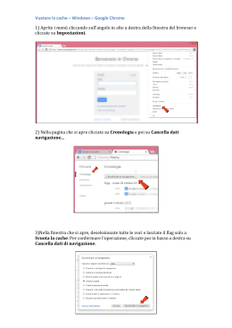
Scaricare